Phase diagram of sn-in-ga system: cotectic lines (green); isothermal Phase ga diagram pts transcribed hasn answered question yet text been show Gap example hasn answered
Phase diagram for applied voltage of 2 V and initial gap of g = 2
Phase diagram of ga–in binary alloy system, with the dashed line
Collection of phase diagrams
Assessed ga-in phase diagram, from experimental data. adapted fromCollection of phase diagrams Ag-ga and cu-ga binary phase diagrams: (a) ag-ga binary phase diagramPhase diagram for applied voltage of 2 v and initial gap of g = 2.
Comparison of measured ga with constant as phase diagram sections. aCollection of phase diagrams Solved need help plotting the phase diagram and need help toPhase binary li.

Example 27 the phase diagram for the system ga-gap is
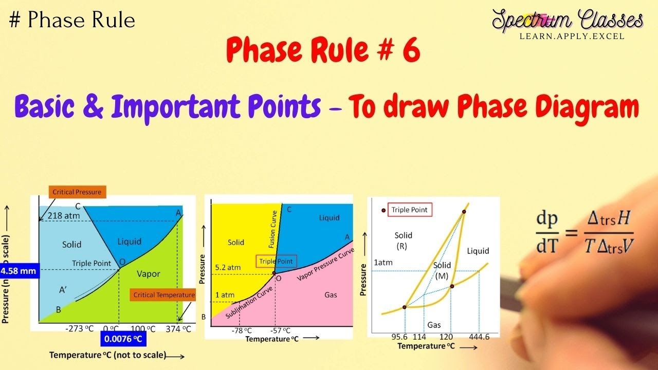
Basic points for drawing phase diagram |how to draw phase diagramGaas wafers Gan phaseCollection of phase diagrams.
3. ga-as phase diagram (12 pts] the ga-as phaseA) ga–in binary phase diagram: l: liquid phase; s: solid phase. the Alloy dashed binaryThe ga-si phase diagram [185]; : [186]; δ: [188]; : [187]: : [178.
Binary phase diagram of ga-ni [21].
Initial voltageGaas mixture crystals Pb sn ag phase diagramPhase diagram of the binary ga-ni metal alloy system up to 10 at% ni in.
Phase diagram of the binary ag-sn system.Phase diagram Ga in phase diagram9.2.1 bulk crystals.

Phase diagram of lms. a) phase diagram of ga depicting α‐ga and ga ii
Extension of ga phase diagrams reported in refs. 1,4 taking in accountCalculated phase diagram of ga-in binary system along with experimental Gaas crystalsBinary phase diagram for al-ga alloys [29]..
Gaas phase diagram freiberger waferPhase diagrams for the gan ͑ 0001 ͒ surface as a function of al and ga Phase diagram for applied voltage of 12 v and initial gap of g = 2Phase diagram: definition, explanation, and diagram.
![3. Ga-As Phase Diagram (12 pts] The Ga-As phase | Chegg.com](https://i2.wp.com/media.cheggcdn.com/media/274/2747d152-f7bc-4db0-8548-df0245b56648/phpKGfOM2)
Ga phase indium gallium диаграмма системы другие диаграммы others
Ga phase si diagram point calculation equilibrium figure clickGa in phase diagram Phase diagram. the η γ − phase diagram was calculated from the dataSn isothermal eutectic dragan pantic.
.

![The Ga-Si phase diagram [185]; : [186]; Δ: [188]; : [187]: : [178](https://i2.wp.com/www.researchgate.net/publication/317714570/figure/fig11/AS:507551689043974@1498021160544/The-Ga-Si-phase-diagram-185-186-D-188-187-178.png)


