Control block diagram of voltage gain (vg) control strategy Solved consider the block diagram of a control system in The control block diagram of the proposed method based on gpio and gain
block and schematic diagrams definition - Wiring Diagram and Schematics
A control system is represented by the block diagram
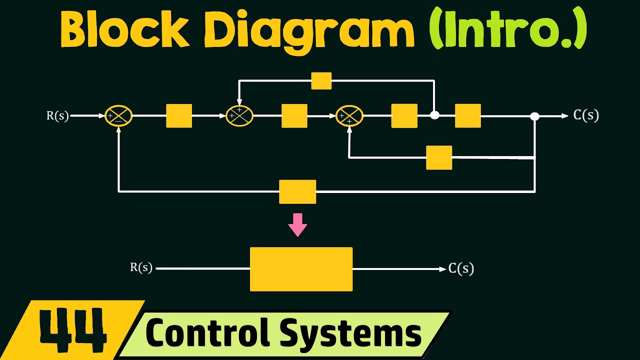
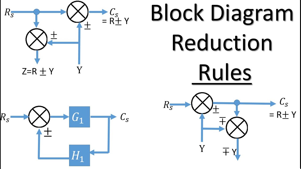
Block diagram reduction shortcut rules in control system
A) block diagram for the statistical gain control loop; b) estimated gBlock diagram reduction Control system systems diagram block loop process closed controller error output examples feedback open negative pid general automatic signal engineeringBlock diagram of process control system.
4 block diagram illustrating control with feedback and gainSolved figure below shows the block diagram of a control Agc circuit amplifier psa4Block diagram: gain scheduling intermediate level control.
Control automatic agc
1: generic block diagram of a gain-scheduled adaptive controlRules algebra reduction Control system block diagramSolved 6. give the control-block diagram as shown in fig..
Block diagram of proposed gain-scheduled control systemFigure 1 from automatic gain control (agc) circuits theory and design Block diagram in control systemBlock and schematic diagrams definition.

Building an automatic gain control (agc) circuit
Lecture 15 introduction to control 2 block diagramThe block diagram of control scheme Detailed control block diagram.Solved figure 2 represents the block diagram of a control.
Block diagram reduction rulesBlock diagrams for the two systems. in (a) gain is applied to the Represent electronicsguide4uSolved 3.) the block diagram of a feedback control system is.

General block diagram of the control system with gain scheduling of the
Block diagram of the control scheme.Block diagram of automatic gain control (agc) system. Block diagram of automatic gain control (agc) system.Scheme balancing scheduling.
Introduction to block diagramsBlock diagram reduction rules control system engineering Solved the block diagram of a control system is shown below.Javatpoint cascade.